화성 EUV라인∙신규 라인 등 파운드리 투자 지속 추진
R&D/제조 전문인력 1만 5천명 채용 및 42만명 간접 고용 효과 예상
삼성전자가 2030년까지 시스템 반도체 분야 연구개발 및 생산시설 확충에 133조원을 투자하고, 전문인력 1만 5천명을 채용한다고 24일 밝혔다.
이는 삼성전자가 2030년까지 메모리 반도체 뿐만 아니라 시스템 반도체 분야에서도 글로벌 1위를 달성하겠다는 '반도체 비전 2030'을 달성하기 위한 것이다.
삼성전자는 또한 시스템 반도체 인프라와 기술력을 공유해 팹리스(Fabless, 반도체 설계 전문업체), 디자인하우스(Design House, 설계 서비스 기업) 등 국내 시스템 반도체 생태계의 경쟁력을 강화할 방침이다.
삼성전자는 과감하고 선제적인 투자와 국내 중소업체와의 상생협력을 통해 한국 시스템 반도체산업 발전에 앞장설 계획이다.
◆시스템 반도체(파운드리 및 시스템LSI 사업) 분야에 133조원 투자, 1만5천명 직접고용
삼성전자는 시스템 반도체 사업경쟁력 강화를 위해 2030년까지 국내 R&D 분야에 73조원, 최첨단 생산 인프라에 60조원을 투자한다.
R&D 투자금액이 73조원 규모에 달해 국내 시스템 반도체 연구개발 인력 양성에 기여할 것으로 기대되며, 또한 생산시설 확충에도 60조원이 투자돼 국내 설비/소재 업체를 포함한 시스템 반도체 생태계 발전에도 긍정적인 영향이 예상된다.
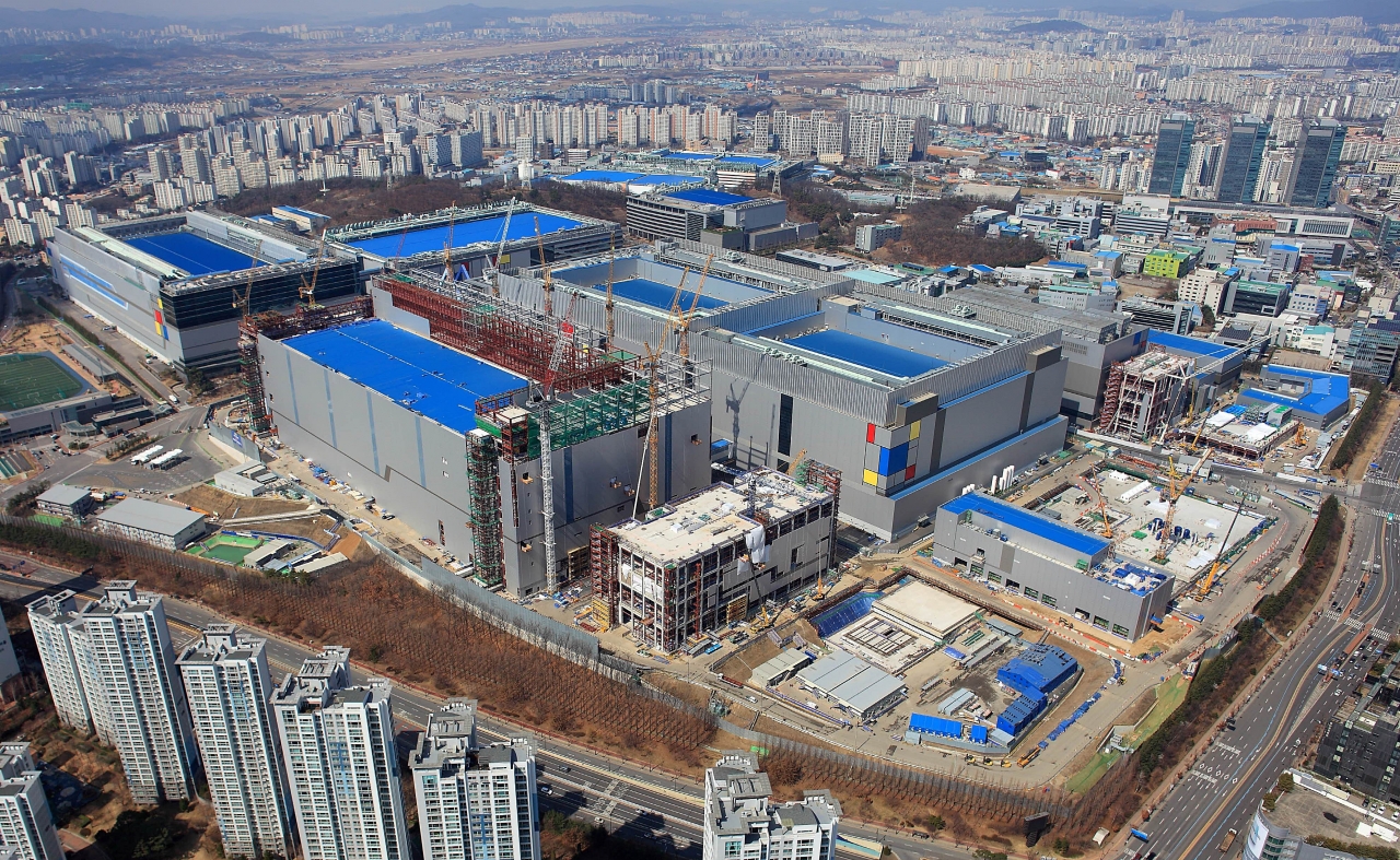
삼성전자는 향후 화성캠퍼스 신규 EUV라인을 활용해 생산량을 증대하고, 국내 신규 라인 투자도 지속 추진할 계획이다.
삼성전자는 또 기술경쟁력 강화를 위해서 시스템 반도체 R&D 및 제조 전문인력 1만 5천명을 채용할 계획이다.
삼성전자의 이 같은 계획이 실행되면 2030년까지 연평균 11조원의 R&D 및 시설투자가 집행되고, 생산량이 증가함에 따라 42만명의 간접 고용유발 효과가 발생할 것으로 예상된다.
◆국내 중소 반도체업체 협력 통해 국가 시스템 반도체 산업생태계 강화
삼성전자는 국내 팹리스 업체를 지원하는 등 상생협력을 통해 한국 시스템 반도체 산업생태계를 강화한다.
국내 중소 팹리스 고객들이 제품 경쟁력을 강화하고 개발기간도 단축할 수 있도록 인터페이스IP, 아날로그 IP, 시큐리티(Security) IP 등 삼성전자가 개발한IP(Intellectual Property, 설계자산)를 호혜적으로 지원한다.
또한, 보다 효과적으로 제품을 개발할 수 있도록 삼성전자가 개발한 설계/불량 분석 툴(Tool) 및 소프트웨어 등도 지원할 계획이다.
소품종 대량생산 체제인 메모리 반도체와 달리 다품종 소량생산이 특징인 시스템 반도체 분야의 국내 중소 팹리스업체는 지금까지 수준 높은 파운드리 서비스를 활용하는데 어려움이 있었다.
삼성전자는 이러한 어려움을 해소하기 위해 반도체 위탁생산 물량 기준도 완화해, 국내 중소 팹리스업체의 소량제품 생산을 적극적으로 지원할 계획이다.
또한 국내 중소 팹리스 업체의 개발활동에 필수적인 MPW(Multi-Project Wafer)프로그램을 공정당 년 2~3회로 확대 운영한다.
삼성전자는 국내 디자인하우스 업체와의 외주협력도 확대해 나갈 계획이다.
[Focus] Samsung Electronics invested 133 trillion won into system semiconductors and started 'Solidarity 2030'
Samsung Electronics Co. said Monday that it will invest 133 trillion won by 2030 in expanding research and development and production facilities in the system semiconductor sector, and hire 15,000 professionals.
The move is aimed at achieving the "Solidarity Vision 2030" that Samsung Electronics aims to achieve the No. 1 global ranking in system semiconductors as well as memory chips by 2030.
Samsung Electronics is also planning to strengthen the competitiveness of South Korea's system semiconductor ecosystem such as Fabless (Fabrication, Semiconductor Design Company) and Design House (Design House, Design Service Company) by sharing system semiconductor infrastructure and technical skills.
Samsung Electronics plans to take the lead in the development of the Korean system semiconductor industry through bold and preemptive investment and win-win cooperation with local small and medium-sized companies.
∘ Investment of 133 trillion won in system semiconductors (foundry and system LSI business) and direct employment of 15,000 workers
Samsung Electronics will invest 73 trillion won in R&D and 60 trillion won in state-of-the-art production infrastructure by 2030 in order to strengthen competitiveness in its system semiconductor business.
It is expected that R&D investment will amount to 73 trillion won, which will contribute to fostering R&D personnel for systems, semiconductors and research and development in South Korea, and 60 trillion won will also be invested in expanding production facilities, which will have a positive impact on the development of system semiconductor ecosystem, including domestic facilities and materials companies.
Samsung Electronics is planning to increase output by utilizing new EUV line of Hwasung campus in the future and continue to invest in new lines in South Korea.
Samsung Electronics also plans to hire 15,000 personnel specializing in system semiconductor R&D and manufacturing to strengthen its
Samsung Electronics' plan, if implemented, is expected to carry out an annual R&D and facility investment of 11 trillion won by 2030, with the indirect employment inducement effect of 420,000 people as production increases.
∘ Strengthening the national system semiconductor industry ecosystem by cooperating with small and medium-sized semiconductor companies in Korea
Samsung Electronics is going to strengthen South Korea's system semiconductor industry ecosystem through win-win cooperation by supporting South Korean fabless businesses.
To help small and medium fabless customers in South Korea strengthen their competitive edge in products and shorten development period, Samsung Electronics' IP (Intelual Property, Design Asset) such as Interface IP, Analog IP, and Security IP will be supported in a reciprocal manner.
It will also support Samsung Electronics' design/defective analysis tools and software to help it develop products more effectively.
Unlike memory semiconductors, which are small- and medium-sized South Korean fabless businesses that are characterized by small variety of production, it has been difficult to utilize high-quality foundry services.
To address these difficulties, Samsung Electronics is also planning to actively support small- and medium-sized South Korean fabless companies by easing standards for consignment production of semiconductors.
In addition, MPW (Multi-Project Wafer) programs, which are essential for development activities of small and medium fabless companies in South Korea, are expanded to two to three times a year.
Samsung Electronics is also planning to expand outsourcing cooperation with South Korean design house companies.